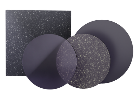
World-Leading Lab-Grown Diamonds, Breaking the Limits of Thermal Management, Optics, and Quantum Computing
Karia Advanced CVD Diamond Materials
- Introduction
-
Headquartered in the US, Karia Technologies is a world-leading manufacturer of lab-grown CVD (Chemical Vapor Deposition) diamonds, dedicated to providing advanced materials for the most demanding technological applications.
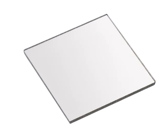
Core process advantages breaking industry standards: Its Single-Crystal Diamond boasts a thermal conductivity of up to 2000~2200 W/m·K, approximately 5 times that of traditional copper. Furthermore, Karia has overcome the size limitations of single-crystal growth, offering monolithic wafers up to 25×25 mm—the largest commercially available, non-mosaic single-crystal specification on the market.
Surpassing the physical limits of traditional materials, Karia is committed to resolving technical bottlenecks in AI computing, next-generation semiconductors, high-frequency communications, and frontier science. We adhere to the highest quality standards; every dispatched diamond product (whether substrate, optical window, or powder) is accompanied by a comprehensive Certificate of Analysis (CoA) and related physical and thermal inspection reports, providing the most reliable data support for your engineering validation.
- Download
- Welcome to download the Karia CVD Diamond product brochure to explore detailed physical property parameters and application cases.
Heat Sinks & Spreaders: Specifically designed for AI GPUs, laser diodes, and RF amplifiers. Offers extreme thermal conductivity up to 1200–1800 W/m·K (polycrystalline) and up to 2200 W/m·K (single-crystal)—up to 12 times the cooling efficiency of copper. Plug-and-play metallization coatings (Ti/Pt/Au, etc.) are available.
Semiconductor Substrates: Flagship Type IIa single-crystal and polycrystalline CVD diamond wafers. Featuring a 5.47 eV wide bandgap, it is the ultimate thermal management platform for GaN-on-Diamond transistors, high-voltage power electronics (tolerating junction temperatures over 400°C), and advanced epitaxial growth.
Quantum Diamonds: Through precisely controlled Nitrogen-Vacancy (NV) centers, these provide millisecond-level T2 coherence times. High-purity isotope options (12C ≥ 99.99%) are available, serving as core materials for room-temperature quantum sensing, quantum communication, and medical single-cell biology research.
Boron-Doped Diamond (BDD): Precisely controlled p-type semiconductor doping grants the diamond excellent electrical conductivity. It possesses the widest electrochemical window (3.5V) among all electrode materials and extremely low background noise. Widely used in neural implants, challenging water treatment, environmental sensors, and superconducting quantum devices.
Optical Windows: A single material covering an ultra-wideband transmission from UV to Far-Infrared (0.22–2500 µm). Combining extreme hardness and chemical resistance, it is the preferred protective window for high-power CO2 lasers, FLIR thermal imaging, synchrotron beamlines, and aerospace sensors.
Diamond Powders: High-precision synthetic diamond powders with particle sizes ranging from 0.1 µm to 500 µm. Available in pure diamond or with nickel, titanium, or resin coatings. Suitable for semiconductor CMP polishing, high-performance Thermal Interface Material (TIM) fillers, and high-strength precision grinding and cutting tools.